

Samsung Introduces World’s First HB RAM With Integrated AI Processing
Posted by MAHNOOR NADEEM
Yesterday, Samsung Electronics announced that it has developed the industry’s first High Bandwidth Memory (HBM) integrated with artificial intelligence (AI) processing power.
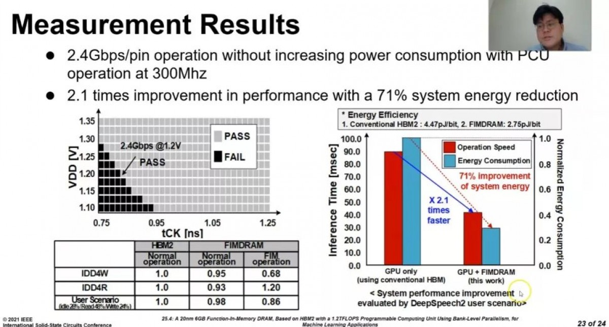
The chipset, called HBM-PIM, comes with a new processing-in-memory (PIM) architecture that, according to Samsung, will deliver over twice the system performance and reduce energy consumption by more than 70%.
The HBM-PIM brings powerful AI computing capabilities inside high-performance memory, to accelerate large-scale processing in data centers, high-performance computing (HPC) systems, and AI-enabled mobile applications.
ALSO READ
Samsung Galaxy A52 4G and 5G Leak in Full Detail Weeks Before Official Launch
For those who don’t know, most of the computing systems today are based on the von Neumann architecture that uses separate processor and memory units to carry out millions of intricate data processing tasks. This approach requires the data to move back and forth between the two units. This results in a system-slowing bottleneck, especially when handling ever-increasing volumes of data.
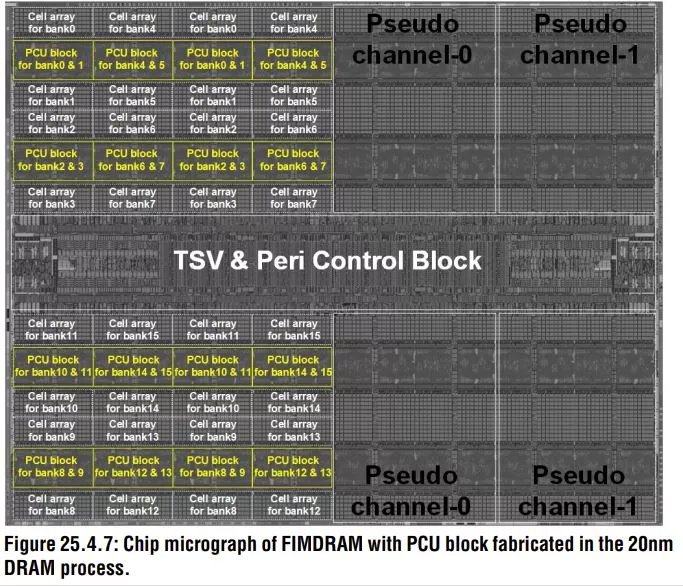
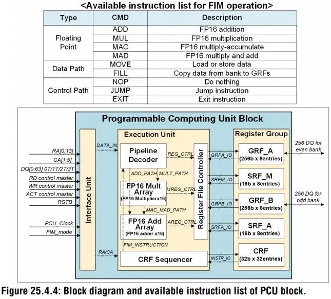
Reportedly, the HBM-PIM will solve this issue since it brings processing power directly to where the data is stored by placing a DRAM-optimized AI engine inside each memory bank called a storage sub-unit. This enables parallel processing and minimized data movement. Moreover, this new architecture does not require any software and hardware changes.
ALSO READ
Samsung Galaxy Book Pro Specs Leak Before Launch
Samsung has managed to get the PCUs working at 300 MHz, which works out to 1.2 TFLOPS processing power per chip. The power usage per chip is kept the same while transferring data at 2.4 Gbps per pin but the overall system energy consumption drops by 71%.
The post Samsung Introduces World’s First HB RAM With Integrated AI Processing appeared first on .


