

Samsung and IBM Announce Breakthrough in Chip Technology
Posted by AASIL AHMED
Samsung and IBM have made a breakthrough in semiconductor chip technology. During the IEDM conference in San Francisco, the two companies unveiled a new design for stacking transistors vertically on a chip, which should greatly improve power efficiency and performance.
Current processors and SoCs have their transistors flat on a surface and the electric current flows from side to side. But with Samsung and IBM’s new Vertical Transport Field Effect Transistors (VTFET) design, transistors sit on top of each other and the current flows vertically.
The VTFET design allows for a greater density of components on a chip compared to current technology. The two companies claim that this should double the performance and improve power efficiency by 85% compared to chips designed with FinFET transistors.
According to Moore’s Law, the number of transistors present in a dense integrated circuit doubles about every two years. Samsung and IBM hope to extend Moore’s Law beyond the nanosheet threshold and waste less energy.
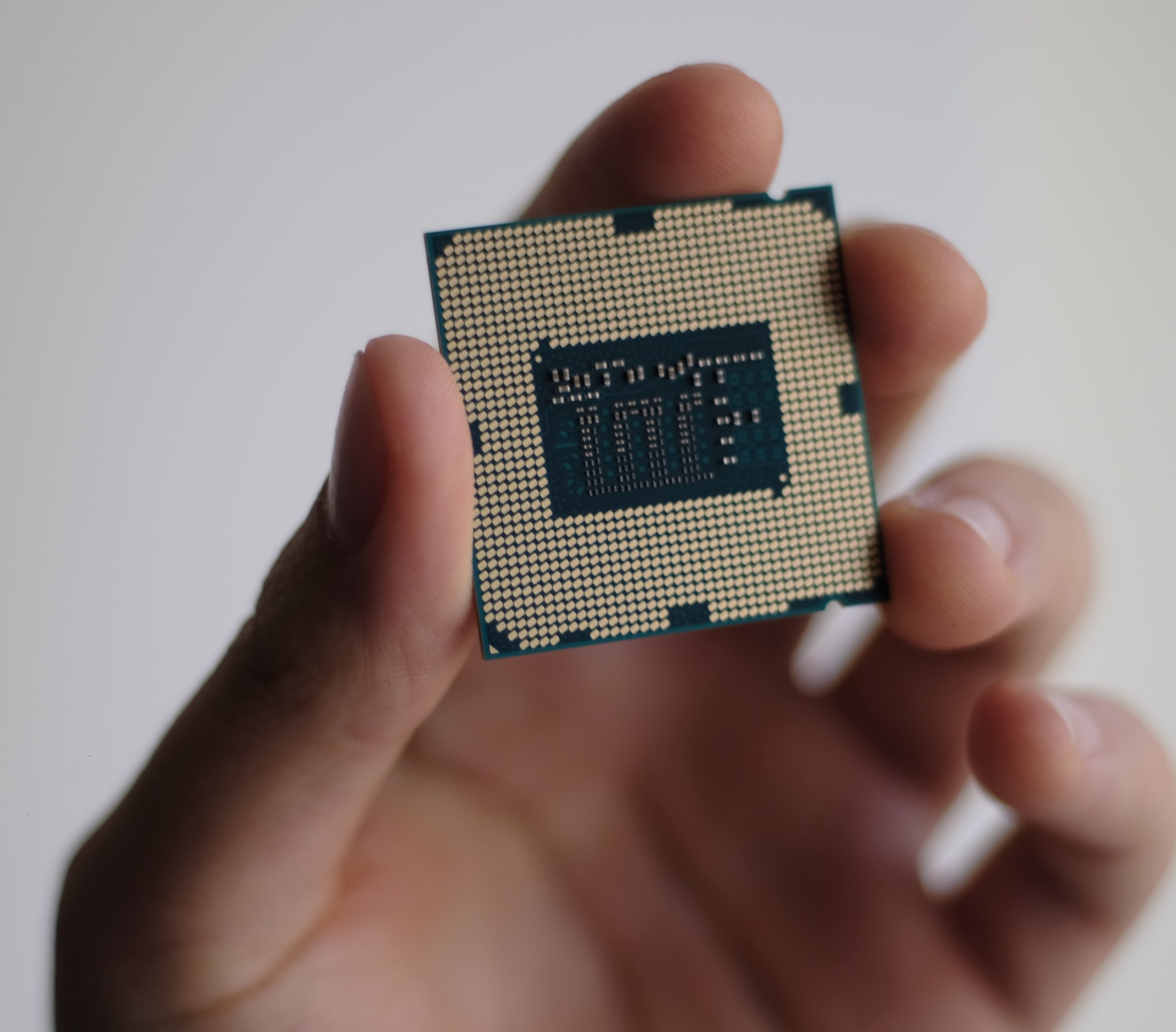
However, Samsung and IBM are not the only ones working on this technology. The American chip manufacturing giant Intel is also looking into chips with transistors stacked above each other to save area, reduce interconnect lengths, and save energy.
Intel is expected to finalize these chips by 2024 using its new “Intel 20A” node and RibbonFET transistors.
The post Samsung and IBM Announce Breakthrough in Chip Technology appeared first on .


